Build-Up PCB
Because of the product enhancement of high integration, PCBs are processed into fine laser drills beyond the limitations of conventional mechanical drills.
This product can be designed in various ways with the free configuration of the drill position according to each layer.
-
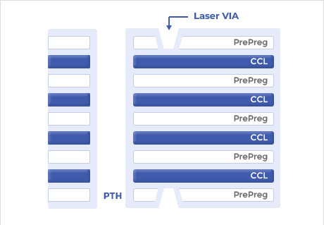
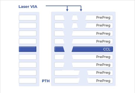
A-TYPE
-
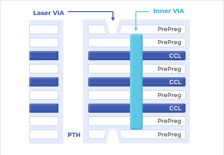
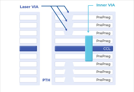
B-TYPE
-
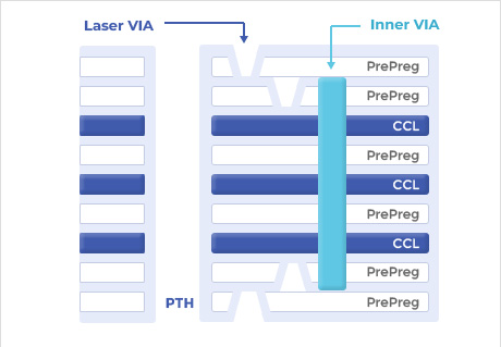
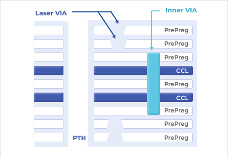
C-TYPE
-
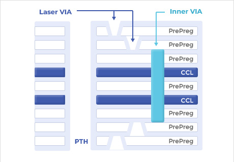
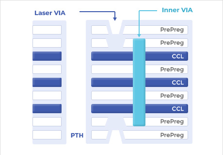
D-TYPE
| A-TYPE | B-TYPE | C-TYPE | D-TYPE | |
|---|---|---|---|---|
| CNC | 1-10 | 1-10, 2-9 | 1-10, 2-9 | 1-10, 3-8 |
| Laser | 1-2, 9-10 | 1-2, 9-10 | 1-2, 2-3, 8-9, 9-10 | 1-2, 2-3, 8-9, 9-10 |
| Stacking count | 1TIME | 2TIME | 2TIME | 3TIME |
Specification
| Item | Capability |
|---|---|
| No. of Layer | 4~12 |
| Board Thickness | 0.4T~1.6T |
| Min Line Width / Space | 0.07mm/0.07mm |
| Min DrILL / Pad | 0.2mm/0.4mm |
| Min Laser Drill / Pad | 0.1mm/0.25mm |